- 您现在的位置:买卖IC网 > Sheet目录479 > MRF24J40MCT-I/RM (Microchip Technology)TXRX MOD 802.15.4 2.4GHZ 12MOD
MRF24J40MC
2.0 CIRCUIT DESCRIPTION
The MRF24J40MC is a 2.4 GHz IEEE Std. 802.15.4?
compliant surface mount module with integrated crystal,
Approval” for a list of tested and approved antenna
types that may be used with the MRF24J40MC
module.
internal voltage regulator, matching circuitry, power
amplifier, low noise amplifier with 50 ? external antenna
2.2
Module Schematic
connector.
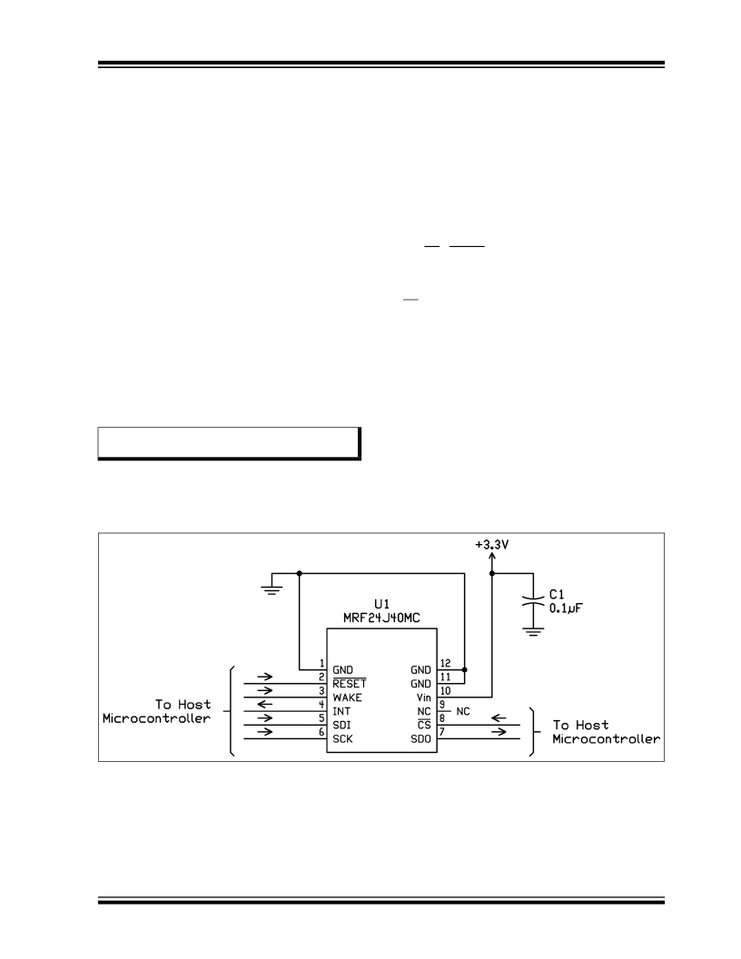
The MRF24J40MC module interfaces to many popular
Microchip PIC microcontrollers through a 4-wire SPI
Interface, interrupt, wake, reset, power and ground. An
A schematic diagram of the module is illustrated in
Figure 2-2 and the Bill of Materials (BOM) is shown in
Table 2-1 .
The MRF24J40MC module is based on the Microchip
example application schematic
is illustrated in
Technology MRF24J40 IEEE 802.15.4? 2.4 GHz RF
Figure 2-1 .
Serial communications and register definitions for the
MRF24J40MC module are documented in the
“ MRF24J40 Data Sheet ” (DS39776). Refer to this
datasheet for specific serial interface protocol and
register definitions. Also, see Section 1.3 “Operation”
for specific register settings that are unique to the
MRF24J40MC module.
Transceiver IC (U6). The Serial I/O (SCK, SDI, SDO
and CS), RESET, WAKE and INT pins are brought out
to the module pins. The SDO signal is tri-state buffered
by U7 to solve a silicon errata, where the SDO signal
does not release to a high-impedance state, after the
CS pin returns to its inactive state.
Crystal, X1, is a 20 MHz crystal with a frequency
tolerance of ±10 ppm @ 25°C to meet the IEEE Std.
802.15.4 symbol rate tolerance of ±40 ppm.
2.1
External Antenna
A balun is formed by components: L11, L12, L13, C25,
The MRF24J40MC module has a 50 ? ultra miniature
coaxial (U.FL) connector to connect to an external 2.4
GHz antenna.
Caution: The U.FL connector is fragile and can only
tolerate very limited number of insertions.
The choice of antenna is limited to the antenna types
the module has been tested with. Refer to the
C27 and C31. L12 is also a pull-up for the RFP and
RFN pins on the MRF24J40. C25 also acts as a DC
block capacitor. RF switches, U1 and U2, switch
between the power amplifier, U3, when transmitting
and low noise amplifier, U2, when receiving. A
band-pass filter FL1 is placed after the PA U3 to reduce
harmonics. The remaining passive components
provide bias and decoupling.
respective country in
Section 3.0 “Regulatory
FIGURE 2-1:
MRF24J40MC APPLICATION SCHEMATIC
? 2011 Microchip Technology Inc.
Preliminary
DS75002A-page 11
发布紧急采购,3分钟左右您将得到回复。
相关PDF资料
MRF49XAT-I/ST
IC RF TXRX 433/868/915 16-TSSOP
MRF89XA-I/MQ
TXRX ISM SUB-GHZ ULP 32QFN
MRF89XAM9A-I/RM
IC TXRX MOD 915MHZ ULP SUB-GHZ
MRX-001-433DR-B
MODULE RECEIVER 433MHZ 18DIP
MRX-002-433DR-B
MODULE RECEIVER 433MHZ 18DIP
MRX-002SL-433DR-B
MODULE RCVR 433MHZ SAW LN 24DIP
MRX-005-915DR-B
MODULE RECEIVER 915MHZ 18DIP
MRX-005SL-915DR-B
MODULE RCVR 915MHZ SAW LN 24DIP
相关代理商/技术参数
MRF24J40T-I/ML
功能描述:射频收发器 2.4 Ghz IEEE/ZigBee transceiver RoHS:否 制造商:Atmel 频率范围:2322 MHz to 2527 MHz 最大数据速率:2000 Kbps 调制格式:OQPSK 输出功率:4 dBm 类型: 工作电源电压:1.8 V to 3.6 V 最大工作温度:+ 85 C 接口类型:SPI 封装 / 箱体:QFN-32 封装:Tray
MRF24WB0MA
制造商:MICROCHIP 制造商全称:Microchip Technology 功能描述:2.4 GHz, IEEE Std. 802.11b? RF Transceiver Module
MRF24WB0MA/RM
功能描述:WiFi/802.11模块 WiFi Transceiver w/PCB antenna
RoHS:否 制造商:Taiyo Yuden 支持协议:802.11 b/g/n 频带: 数据速率:150 Mbps 接口类型:SDIO 传输功率(最大): 天线连接器类型: 工作电源电压:3.4 V to 5.5 V 传输供电电流: 接收供电电流: 最大工作温度:+ 80 C 尺寸:35 mm x 15 mm x 2.9 mm
MRF24WB0MA_13
制造商:MICROCHIP 制造商全称:Microchip Technology 功能描述:MRF24WB0MA/MRF24WB0MB Data Sheet 2.4 GHz IEEE 802.11ba?¢
MRF24WB0MB
制造商:MICROCHIP 制造商全称:Microchip Technology 功能描述:2.4 GHz, IEEE Std. 802.11b? RF Transceiver Module
MRF24WB0MB/RM
功能描述:WiFi/802.11模块 WiFi Transceiver w/uFL connector
RoHS:否 制造商:Taiyo Yuden 支持协议:802.11 b/g/n 频带: 数据速率:150 Mbps 接口类型:SDIO 传输功率(最大): 天线连接器类型: 工作电源电压:3.4 V to 5.5 V 传输供电电流: 接收供电电流: 最大工作温度:+ 80 C 尺寸:35 mm x 15 mm x 2.9 mm
MRF24WG0MA_12
制造商:MICROCHIP 制造商全称:Microchip Technology 功能描述:MRF24WG0MA/MB Data Sheet 2.4 GHz IEEE 802.11b/ga?¢
MRF24WG0MA-I/RM
功能描述:WiFi/802.11模块 PCB ANTENNA RoHS:否 制造商:Taiyo Yuden 支持协议:802.11 b/g/n 频带: 数据速率:150 Mbps 接口类型:SDIO 传输功率(最大): 天线连接器类型: 工作电源电压:3.4 V to 5.5 V 传输供电电流: 接收供电电流: 最大工作温度:+ 80 C 尺寸:35 mm x 15 mm x 2.9 mm
